
Партнерка на США и Канаду по недвижимости, выплаты в крипто
- 30% recurring commission
- Выплаты в USDT
- Вывод каждую неделю
- Комиссия до 5 лет за каждого referral
DT 832 SMD номиналы
Извиняюсь) воть:
№ платы - KT5851 / дата: 08.06.27
6RKOM........
6RKOM........
6R3 - 1 MOM - (SMD - 501)........
6RKOM........
6RR.........
.............................
6C1 - 4 PF..........
6CPF.....
6CPF.....
6CPF.....
6CPF.....
6CPF.....
.............................
6RT KOM - ( SND - 152)....
RX - 100 OM - (SMD - 1000)...
RX 2 - 6 KOM - (SMD - 6001)...
6D1 - любой на ток 2А.......
.............................
6R14 - 9 KOM - (SMD - 9001)...
6R1OM - (SMD - 9000)...
6R1OM - (SMD - 2 X 202)...
6R17 - 1 KOM - (SMD - 1001)...
6R1KOM - (SMD - 5483)...
6R1KOM - (SMD - 3523)...
6R2KOM - (SMD - 9002)...
6R21 - 9 KOM - (SMD - 9001)...
6R2OM - (SMD - 9000)...
6R2KOM - (SMD - 2 X 1002)...
6R24 - 9 OM - (SMD - 9R00)...
6R25 - 1 OM - (SMD - 2 X 1R00)...
6R2KOM...
6R2KOM...
6R2KOM...
6R2KOM...
6R3KOM...
6R3KOM...
Обсуждение конструкций и ремонта DT-832 http://vrtp.ru/index.php?showtopic=15123&st=20
Частотомерная приставка к мультиметру DT-832 | |
Приставка работает с сетевым питанием, поэтому ей можно пользоваться только в стационарных условиях. Чувствительность входа 50 mV, максимальное входное напряжение 30 V. Входное сопротивление не ниже 22 kOm. |
http://forum. /index. php? showtopic=13268&st=180#
Защита и питание мультиметра
Сделай сам ESR (ЭПС) измеритель — приставка к цифровому мультиметру
http://*****/practice/diy-tech/1794-esr-meter-eps-pristavka-k-multimetru. html
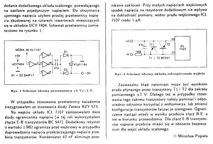
ЭТУ и другие приставки можно попробовать питать от повышающего преобразователя из Р№11, 2001с42 (подробно Р№12 1981с46 и Р№6, 2005)
Статья о приборе для измерения ESR (ЭПС) конденсаторов появилась в журнале «Радио» №8 за 2011 год.
Я повторил эту конструкцию с некоторыми изменениями и хочу поделиться с вами впечатлениями и результатами.
Начало
Да, эта тема многократно обсуждалась, в том числе и здесь. Я собрал два варианта схемы Ludens и они очень хорошо себя зарекомендовали, тем не менее, у всех предлагаемых ранее вариантов есть недостатки. Шкалы приборов со стрелочными индикаторами очень нелинейны и требуют для калибровки много низкоомных резисторов, эти шкалы надо рисовать и вставлять в головки. Приборные головки велики и тяжелы, хрупки, а корпуса малогабаритных пластмассовых индикаторов обычно запаяны и они часто имеют мелкую шкалу. Слабым местом почти всех предыдущих конструкций является их низкая разрешающая способность. А для конденсаторов LowESR как раз надо измерять сотые доли Ома в диапазоне от нуля до половины Ома. Предлагались также приборы на основе микроконтроллеров с цифровой шкалой, но не всякий занимается микроконтроллерами и их прошивками, устройство получается неоправданно сложным и относительно дорогим. Поэтому в журнале «Радио» сделали разумную рациональную схему — цифровой тестер есть у любого радиолюбителя, да и стоит он копейки.
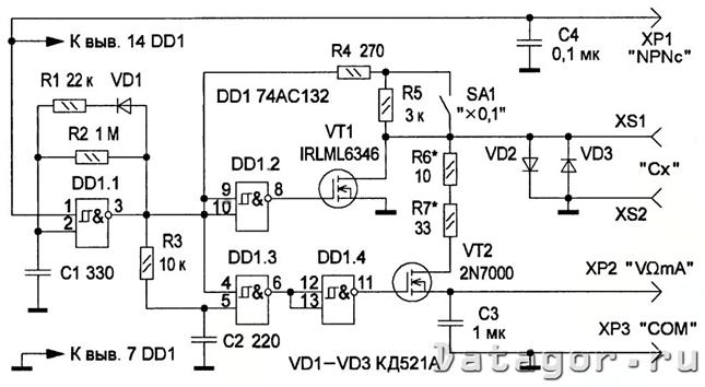
Мой вариант
Я тоже стараюсь делать приборы-приставки к цифровому тестеру — это просто и дёшево. Но в журнальной статье мне не всё понравилось. Например, «…была поставлена задача не применять дополнительный источник питания». Вспоминаются советские времена и выражение «есть мнение». Кто поставил такую дурацкую задачу, журнал умалчивает. Экономия батарейки, которая стоит как трамвайный билет и будет работать год и более? Зачем? Следующая плюха — бескорпусной вариант. Такая конструкция с торчащими штырьками неудобна и должна храниться дома под стеклянным колпаком. Мне больше нравится, когда коробку можно спокойно бросить в сумку с инструментом и поехать «на дело».
Я внес минимальные изменения. Корпус — от неисправного «электронного дросселя» для галогеновых ламп. Питание — батарея «Крона» 9 вольт и стабилизатор 78L05 (на схеме не показан). Убрал переключатель — измерять LowESR в диапазоне до 200 Ом надо очень редко (если приспичит, использую параллельное подключение). Изменил некоторые детали. Микросхема 74HC132N, транзисторы 2N7000 (to92) и IRLML2502(sot23). Из-за увеличения напряжения с 3 до 5 вольт отпала необходимость подбора транзисторов.
При испытаниях устройство нормально работало при напряжении батареи свежей 9,6 В до полностью разряженной 6 В.
Кроме того, для удобства, использовал smd-резисторы. Все smd-элементы прекрасно паяются паяльником ЭПСН-25. Вместо последовательного соединения R6R7 я использовал параллельное соединение — так удобнее, на плате я предусмотрел подключение переменного резистора параллельно R6 для подстройки нуля, но оказалось, что «нуль» стабилен во всем диапазоне указанных мною напряжений.
Удивление вызвало то, что в конструкции «разработанной в журнале» перепутана полярность подключения VT1 — перепутаны сток и исток (поправьте, если я неправ). Знаю, что транзисторы будут работать и при таком включении, но для редакторов такие ошибки недопустимы.
Наладка
Наладка очень проста и заключается в установке чувствительности с помощью R4 при подключенном резисторе 2…5 Ом и установке нуля цифрового вольтметра на диапазоне 200mV.
Операции надо повторить несколько раз, далее можно убедиться в точности измерителя, подключая резисторы 0,1…5 Ом. Настраивать надо со штатными шнурами, плату хорошенько промыть, конденсатор С3 должен быть термостабилен.
К вопросу о точности вообще
Начиная с 10 Ом, точность примерно 3% и ухудшается примерно до 6% при 20 Ом (200мВ), но точность при измерениях бракованных элементов не важна. Поскольку измерения проводятся при комнатной температуре, термонестабильность будет мала, испытаний на эту тему я не проводил.
При измерениях ESR конденсаторов в компьютерных блоках питания и на материнских платах, я пришел к выводу, что конденсаторы от 1000 мкФ с сопротивлением 0,5 Ом надо срочно выпаивать и отправлять в ведро, нормальное ESR 0,02…0,05 Ом. Попутно обнаружил, что у исправных конденсаторов ESR очень сильно зависит от температуры, так у конденсатора 22 мкФ ESR уменьшалась от тепла пальцев на 10%. Это объясняет, почему некоторые фанатичные лампадные конструкторы специально делают подогрев конденсаторов в катодных цепях с помощью проволочных обогревателей. По этой причине, а также по причине имеющегося сопротивления контактов считаю, что в измерения тысячных долей Ом нет особой необходимости.
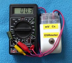
На первом фото ЭПС конденсатора 0,03 Ом.
Желающие подробнее ознакомиться с принципом работы данного устройства могут прочитать оригинальную статью на стр. 19, 20 «Радио» №8 за 2011 год.
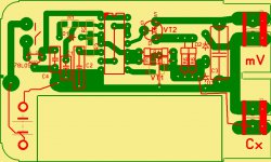
Моя печатная плата
Прилагаю печатную плату в формате LAY. Я стараюсь рисовать дорожки как можно шире, а расстояния между выводами делаю максимальными, не брезгую перемычками (будьте внимательны), если это упрощает изготовление платы.
Итого
Данный прибор работает у меня около месяца, его показания при измерениях конденсаторов с ESR в единицы Ом совпадают с прибором по схеме Ludens.
Он уже прошёл проверку в боевых условиях, когда у меня перестал включаться компьютер из-за емкостей в блоке питания, при этом не было явных следов «перегорания», а конденсаторы были не вздувшимися.
Точность показаний в диапазоне 0,01…0,1 Ом позволила отбраковать сомнительные и не выбрасывать старые выпаянные, но имеющие нормальную ёмкость и ESR конденсаторы. Прибор прост в изготовлении, детали доступны и дёшевы, толщина дорожек позволяет их рисовать даже спичкой.
На мой взгляд, схема очень удачна и заслуживает повторения.
Преобразователь для питания стрелочного мультиметра
http://www. *****/circuit/power/converter/36/
Для питания в режиме измерения сопротивлений в таких приборах используется 4,5В-я батарея. Раньше эти батареи были дешевыми и нормального качества, их хватало надолго. Сейчас их цена сравнивается с ценой на никель-кадмиевые аккумуляторы и качество никакое, при интенсивном использовании режима омметра батареи хватало на неделю, в лучшем случае - на две. Поэтому было решено: берем один никель-кадмиевый аккумулятор типоразмера АА или ААА (у меня ААА) 1,2В и делаем из него 4,5В. Преобразователь сделан на основе схем для питания светодиодов, которых в сети и радиолюбительских журналах огромное количество:
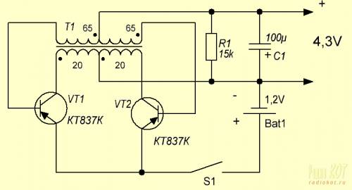
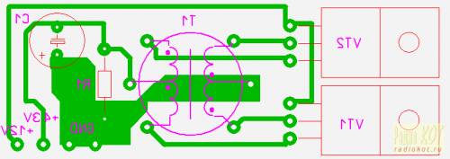
Трансформатор Т1 намотан на кольце из феррита 2000НМ типоразмера К10х6х3. В первичной обмотке 40 витков с отводом от середины, во вторичной - 130 витков с отводом от середины провода диаметром 0,3 мм. Преобразователь смонтирован на простой печатной плате:
При монтаже трансформатора учитывать фазировку обмоток: точки на схеме - начала обмоток. При правильном монтаже и исправных деталях преобразователь начинает работать сразу. Возможно, потребуется подбор резистора R1 для надежного запуска преобразователя без нагрузки. Выключатель S1 монтируем где-то на боковой стенке прибора.
Порядок пользования такой: переключаем прибор в режим измерений сопротивлений, включаем S1, меряем :) После завершения измерений выключаем S1 чтоб не садить аккумулятор. В таком режиме аккумулятора хватает надолго (в моем приборе - где-то на пол-года).
Подобным образом переделал и цифровые мультиметры, так-как 9В-е батареи тоже сейчас никакого качаства. Преобразователь для цифровых мультиметров изпользовал из "РАДИО" №11 2003г., ст. 21 без изменений.
Для LC-метра
http://*****/u1.htm
24.Одновибратор на индуктивности.
25.Одновибратор на индуктивности.
26.Одновибратор на индуктивности и триггере.
Reading inductance with your DC voltmeter or frequency counter
http://sound. /project121.htm
Copyright 2007 Peter H. Lehmann. All Rights Reserved.
Images Redrawn, Edited by and © Rod Elliott (ESP) 2008
var addthis_config = { data_track_clickback: true } var addthis_config = {"data_track_clickback":true}; More Sharing ServicesShare | Share on facebookShare on myspaceShare on googleShare on twitter
Introduction
Commercial choke coils for speaker crossover networks can be costly. Winding your own coils allows you to quickly have whatever size of coil you want while spending very little on enamelled wire and a former. Finding an inexpensive way to measure inductance can further the appeal of winding your own. Both of the two separate inductance-metering circuits described here can be quickly assembled from readily available and low-cost parts.
The availability of inductance meters for a moderate price should be kept in mind. In the spring of 2007 I found three inductance meters on the Web at an advertised price of about US$50 each. Range and accuracy of the commercial meters would be better than that of the two circuits described here.
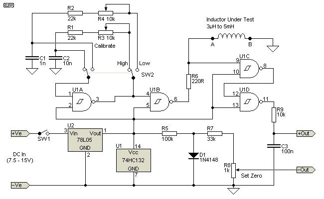
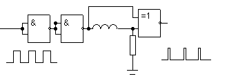
Figure 1 - Inductance Adaptor (Kit Version, With Design Flaws)
Figure 1 shows the schematic diagram of an "adapter" that I purchased as a kit. This circuit has design flaws that substantially degrade accuracy. Thus the circuit as shown in Figure1 shouldn't be built... but it can be modified as described here to operate as originally intended.
The circuit is intended to produce a DC output voltage VOUT directly proportional to inductance of L1. Setting the adapter for measuring inductance in a low range, VOUT in millivolts is directly read as microHenries. Switched for measuring inductance in a high range, VOUT in millivolts is read as milliHenries after moving the decimal point two places to the left.
Linear positive voltage regulator U2 is included to provide a steady +5V for IC U1. Regulator U2 is needed as VOUT varies directly with the power supply voltage, and IC U1 will not withstand a supply voltage above 7V.
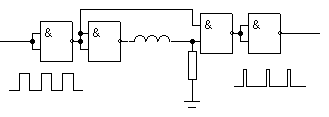
IC U1 is a quad two input Schmitt NAND gate. All fours gates of U1 are configured as inverters. That is, one of the two input pins of each gate (pins 2, 5, 10 and 13) is connected to Vcc.
Gate U1A is configured as a multivibrator oscillator by connecting feedback resistance from output pin 3 to input pin 1 and a capacitor from input pin 1 to ground. With DPDT switch S2 positioned as shown for measuring inductance in a high range, the period of oscillation of the oscillator is equal to about 66% of the time constant (R1 + R3) * C2. Capacitance of C1 is 0.1 of C2 and (R2 +R4) = (R1 + R3). Thus switch S2 alternately positioned for measuring inductance in the low range decreases the period of oscillation by about 1/10th.
The output (pin 3) of the oscillator is connected to input pin 4 of U1B, buffering the oscillator from the next operation of the quad gates. Resistor R6 is connected from output pin 6 of U1B to input pin 9 of U1C. The coil under test is connected from pin 9 to ground.
Of special concern is the input protection that is provided at all of the input pins of U1. A typical equivalent of the type of integrated input protection included on the most CMOS ICs is shown in Figure 1a. The diodes prevent voltage either greater than Vcc or negative with respect to ground from damaging the fragile input gate structure of the MOSFET transistor in the IC. How the input protection at pin 9 affects operation of the adapter will be explained in a following section.
Closing power switch S1, the voltage taken at pin 9 of U1C alternates between high and low states. Output pin 8 of U1C is connected to pin 12 of U1D. Thus the output on pin 11 switches high and low following the signal at pin 9.
Resistor R9 in series with capacitor C3 is connected from output pin 11 of U1D to ground. The ratio of the time that pin 11 remains high with respect to the time interval set by the oscillator is the duty cycle. The voltage drop across C3 (VOUT) is directly proportional to duty cycle, provided that the voltage remains below 1V.
Resistors R5 and R7, trimpot R8 and diode D1 provide for zeroing VOUT when pin 9 of U1C is shorted to ground. Resistor R5 connected in series with D1 from pin 1 of the regulator to ground limits current through diode. R7 and pot R8 connected across the terminals of diode D1 form a voltage divider. Reading VOUT of the adapter is accomplished by connecting the positive and common leads of a DVM between the junction of R9 and C3, and the wiper of pot R8.
Calibrating The Figure 1 Adapter
Following the instructions that came with my kit, the first step is to zero VOUT by grounding input pin 9 of U1C and adjusting the setting of R8. With input pin 9 at ground, there is a negligible voltage drop across capacitor C3. Thus I came to the conclusion that the zeroing circuitry of the adapter of Figure 1 doesn't serve a useful purpose. This may not necessarily be the case, as CMOS outputs may have a small residual voltage when at logic zero. Use of the diode is ill advised however. ![]()
With pin 9 grounded, the output at pin 11 of U1D is held low... virtually at ground. The output stage of U1D in the output low state can be modelled as pin 11 connected by a non-conducting p-channel MOSFET to +V and by a conducting n-channel MOSFET to ground. The p-channel connecting pin 11 to +V is essentially an open circuit and only the negligible current of capacitor C3 discharging flows through resistor R9 in series with the low resistance of the n-channel connecting pin 11 to ground. With a very small voltage drop across the n-channel there is no output offset voltage to be compensated. Thus my modified version of the adapter of Figure 1, shown in Figure 3, does not include any zeroing circuitry.
The second step in calibrating the adapter is setting the period of oscillation of the relaxation oscillator to cause VOUT to correctly correspond to inductance of the calibration coil. For measuring in the high range of 100uH to 5mH with switch S2 set as shown, the instructions that came with my kit said to use 5mH, and adjust trimpot R3 until VOUT reads 500mV.
With switch S2 set to the low range, the adapter is able to measure inductance in the range of 3uH to 500uH. For calibration, a test inductor of 400uH is used, and trimpot R4 is adjusted until VOUT equals 400mV.
Inductance & Duty Cycle
U1 is a quad Schmitt trigger NAND gate. Each input terminal of the gates of U1 has an upper and lower threshold voltage. With Vcc of 5V, the threshold voltages are about 3V (VH) and 2V (VL). The voltage applied to pin 9 of U1C is determined by the inductance of the test inductor. The inductor has a time constant that is proportional to the inductance. When voltage is applied, the inductor resists the current change, and voltage rises to Vcc. During this time, the output of U1C is low. As current starts to flow, the voltage across the inductor falls until the lower threshold is reached, and the output of U1C switches high. See Figure 2a below for the waveform.
Pin 6 of U1B presents a square wave, with a peak-to-peak voltage very close to Vcc and ground. This is supplied to the coil under test via the 220 ohm resistor (R6). The frequency of the multivibrator based on U1A is adjusted using R3 or R4 (depending on range) so that the reading at the output is correct for the value of test inductance. The duration of pin 11 of U1D being held high is directly proportional to the inductance of the coil.
The differential of the squarewave voltage from pin 11 is directly proportional to the duty cycle of the waveform generated across the test inductance, and is therefore directly proportional to the value of the inductor. Following calibration of the adapter, the oscillation frequency for each measuring range is fixed.
Difficulties With The Kit Adapter
One of the difficulties that I encountered in using the adapter kit was a fluctuating DC output. I traced this problem to the kit circuit lacking capacitors C4 and C5 shown in Figure 3. These capacitors are recommended in regulator data sheets for linear regulators when the regulator is located at a distance from the power supply filter capacitors. (In fact, the data sheets generally recommend that bypass caps are always used, and I do not recommend that they ever be omitted ![]() ).
).
I found that only a very little spacing of the 78L05 regulator from a power supply or battery without the attached stabilising capacitors causes instability and usually reduced the output voltage of the regulator. Connecting a 78L05 regulator to a standard 9V battery by means of a clip with 150mm leads and loading the regulator with a resistive load for a current of 10mA, the output voltage fell to 4V.
Even after fixing the problem of the regulator output being lower than it should be, I was unable to calibrate the adapter for measuring in the high range with a 5mH inductor. Even decreasing the resistance of trimpot R3 to zero, VOUT only increased to a maximum of about 400mV. Next I tried R1 reduced to 12k. With the revised R1 in place, decreasing resistance of trimmer R3 from maximum resistance setting caused VOUT to decrease from a maximum of about 400mV. According to the instructions that came with the kit, I should have been able to adjust trimmer R3 to produce VOUT of 500mV.
With the help of an oscilloscope, I eventually discovered that decreasing the period of oscillation resulted in an output low (at pin 6) period of insufficient duration for all of the energy stored in the coil field to be dissipated via R6. The energy stored in the field of the test coil is dissipated when pin 6 of U1B switches to ground. When the output goes high again, a voltage still exists across the coil.
It is worth noting that D1 is a very bad idea. Because diodes have a significant temperature coefficient, the voltage across R8 will vary with temperature. While such a variation could conceivably be used to compensate for the temperature variation in the CMOS output stage, it seems highly unlikely that this was the original intention. Since the original designer was unaware that linear regulators need bypass caps, it is probable that s/he was also unaware of the -2mV/°C of silicon diodes. If the idea was to form a stable low voltage reference (which is almost certainly the case), it fails there too, because the forward current is much too low ![]()
Coil Waveform
When pin 6 of U1B goes low, this starts the collapse of the inductor's magnetic field. Resistor R6 dissipates the energy stored in the field. The back EMF of the inductor is negative with respect to ground.
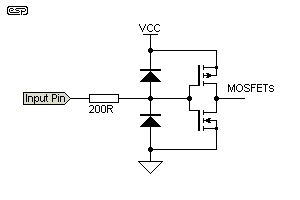
Figure 2 - Equivalent Circuit of CMOS Input Stage
When the coil voltage is negative with respect to ground, the lower diode in the input protection circuit shown above conducts. This changes the charge/discharge behaviour of the coil and prevents the field from collapsing fully.
Failure to use any external resistance also stresses the CMOS input stage unnecessarily.
If the coil's magnetic field is not given sufficient time to collapse (or a protection diode causes additional loading), a negative voltage exists across the coil, which adds to the positive voltage applied from the test circuit. When a positive and negative value are added, the result is a lower positive voltage than expected. Any voltage that remains across the coil therefore creates a real problem. This can easily be sufficient to prevent U1C from detecting the positive to negative-going transition reliably (see Figure 2a) ... if at all.
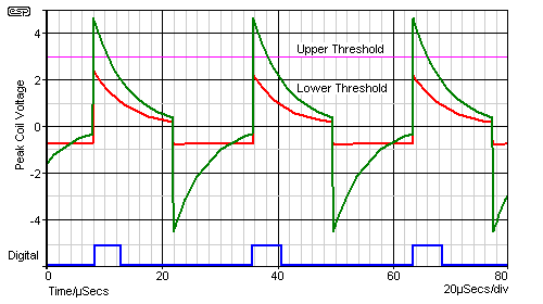
Figure 2a - Waveform With Diode (Red) and Without Diode (Green)
As you can see, a diode in the circuit will prevent the peak voltage from ever reaching the upper Schmitt trigger threshold. For clarity, no resistance was used in series with the diode, but the effect with resistance is very similar (although not as pronounced). Because the coil's field does not collapse fully, the full 5V pulse voltage never appears across the coil, the Schmitt trigger cannot detect the transition, and this limits the measurement range and reduces the linearity and accuracy.
In order for a Schmitt trigger to do anything, the input voltage must first exceed the upper threshold (the output will then switch low). When the voltage falls below the lower threshold, the trigger circuit then switches the output high again. If the upper threshold is never reached, the output will never switch low. A residual coil voltage will affect the duty cycle of the output waveform, and therefore the accuracy of the instrument.
Look at the blue trace. This is the digital output (not to scale) expected from the output of U1D (pin 11), and is based on the green trace which passes through both Schmitt thresholds as it should. The red trace will leave pin 11 at ground permanently. Somewhere in between the extremes of the red and green traces, it is obvious that the pulse width will be much narrower than it should be.
Note however, even the green trace shows that the voltage has not returned to zero before the next pulse arrives. This is exactly the problem that Peter referred to above. While the error cause by the small offset visible on the green trace will not be large, it is still an error.
As shown, the green trace stops and starts about 40mV below and above the zero volt line respectively. For accurate readings, this residual voltage should be as small as possible. As shown in Figure 2a, the green trace represents the absolute upper limit of inductance for a given frequency. A higher inductance or frequency will not produce a corresponding or accurate measurement beyond this limit. While it might be expected that more inductance would give a higher reading, the output voltage at the measurement terminals will actually fall with increased inductance. ![]()
Improved Inductance Meter
Compared to the adapter of Figure 1, my revised adapter has simplified construction and a reduced parts count by being configured to measure inductance in the single range of 200uH to 5mH. This range is the one that would be used for measuring choke coils for speaker crossover networks which was my main concern.
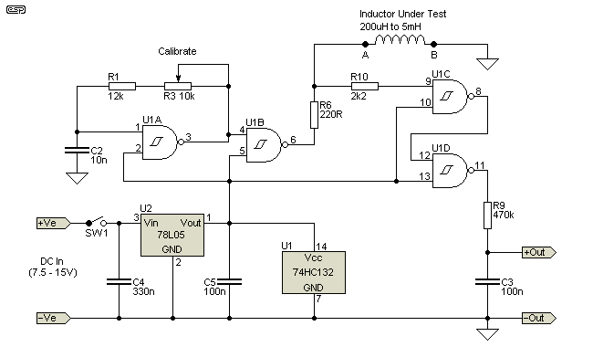
Figure 3 - Improved Inductance Adaptor
My revisions to the adapter of Figure 1 include the new resistor R10 that makes it possible to calibrate it to read VOUT = 500mV corresponding to known L1 = 5mH. With output pin 6 of inverter U1B residing at ground, VL1 is negative with respect to ground causing the input protection diode D3 of Figure 2 to conduct. Thus the back EMF of the coil has two parallel current paths to ground through resistors R6 and R10. As resistor R10 is ten times the value of R6, the time constant for energy dissipation of the inductor's stored charge is L1 / R6. Without the offset created by the protection diode, the period of the oscillator can be shortened sufficiently to obtain a correct reading. The period will normally be several time constants, to allow sufficient time for the coil voltage to return to zero.
Additionally my adapter includes increasing R9 from 10kOhm to 470kOhm. Making R9 = 470k reduced "drooping" or consistently low readings at VOUT with respect to L1 of known inductance < 3mH. This improved accuracy can probably be attributed to increasing the time constant R9*C3 and reducing low output voltage taken at output pin 11 of inverter U1D - equal to a few mV with VOUT equal to several hundred millivolts. I found that with R9 equal to the original value of 10k, increasing capacitor C3 to 10uF did not reduce non-linearity of the adapter.
Alternate Version ![]()
An alternate version of the "Improved Inductance Adaptor" is shown below. The main reason I added this was to ensure that the somewhat limited output current from CMOS logic would be able to drive the test coil with sufficient current to ensure that the current limit is imposed by the resistor (R3) and never by the logic IC itself. The 4584 or 74HC14 CMOS inverting Schmitt trigger are both usually quite easy to obtain, and by paralleling 3 inverters a reasonable output current is assured. It is essential that R4 is mounted as close to pin 11 of U1E as possible, to reduce stray capacitance to the lowest possible value. Simulation shows good linearity and accuracy of better than 4% over the full operating range.
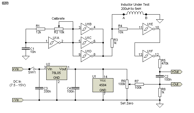
Figure 3a - ESP's Version of Improved Inductance Adaptor
Oscillation frequency with the pot centred is the same as the originals shown above. As you can see, the essential elements are identical to that shown in Peter's version. Operation is also identical, but this circuit should operate up to a higher frequency before non-linearity becomes a problem. This should improve performance with low value inductors, but the circuit has not been built and tested. It may transpire that there is little improvement, but since CMOS logic is limited to around 5mA per output (at best, with a 5V supply) and the 220 ohm resistor demands up to 22mA at 5V, the parallel gates will ensure that more current is available than from a single gate.
For reference, CMOS Schmitt trigger oscillators of this configuration have a frequency that depends on the type of device. The 4584, 74HC14 and 74HCT14 types are all different, and different manufacturers give different formulae for the oscillation frequency. All formulae are approximate at best, and some that I've found are shown below. They show significant variations - and which is closest to reality is rather dubious, especially for the 4584. The symbol ≅ means "approximately equal" ...
- 4f ≅ 1 / ( 0.3 * R * C ) so the median frequency (with R3 centred) is 1 / ( 0.3 * 17k * 10nF ) ≅ 19.6kHz 74HC14 ... f ≅ 1 / ( 0.8 * R * C ) the median frequency is 1 / ( 0.8 * 17k * 10nF ) ≅ 7.35kHz 74HCT14 ... f ≅ 1 / ( 0.67 * R * C ) median frequency is 1 / ( 0.67 * 17k * 10nF ) ≅ 8.78kHz
Please note that the components are renumbered from Peter's versions. I must stress that the version shown here has not been built (I already have two inductance meters), but a simulation does show great promise. According to the simulation, linearity and accuracy remain within 4% to well below 200uH, with the only limitation being the logic zero voltage from the CMOS output (on pin 12). A zero calibration (test coil shorted) will give you a reading of a few millivolts, and this determines the lower limit - any reading less than 10 times the zero reading will not be usably accurate.
It may be necessary to adjust the value of R1 and/or R3 to obtain calibration - this is a variable that can't be estimated, because all CMOS Schmitt trigger ICs are slightly different, even those from the same manufacturing batch. As shown above, the formulae are different for the different CMOS families, and are approximate at best.
Components R6, R7 and R8 are optional. If you find that there is more than a couple of millivolts present at the output, these will provide an adjustable offset so the meter reads zero when the test coil terminals are shorted. If not required, connect C2 (and the - OUT terminal) to ground (-VE supply input terminal). By removing all offset, the circuit will provide good linearity with inductors as small as 50uH (output voltage is 5mV for 50uH) - provided that your meter will give a useful reading for such a low voltage. ![]()
Alternative Inductance Meter
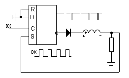
The 555 timer IC configured as an astable multivibrator is (almost) universally shown using the rate of capacitive energy storage and withdrawal providing timing intervals. Here, the energy storage and release of a coil provides the timing intervals. The frequency of the square wave of the timer taken at output pin 3 of IC U2 is inversely proportional to the inductance of L1. Thus reading that frequency indicates the inductance of L1.

Figure 4 - Frequency Meter Inductance Adaptor
Compared to the adapter of Figure 3, the timer has the advantages of being able to accurately measure inductance to 10mH, a lower parts count and calibration with a choke coil of 500uH, which costs substantially less than the 5mH required for calibrating the adapter of Figure 3.
Digital multimeters including a frequency counter are becoming more common, so chances are that you might currently own an appropriate counter. The output frequencies of the timer corresponding to values of inductance of L1 of 500uH and 10mH are respectively 200kHz and 10kHz.
As the timer is calibrated to read an output frequency of 200kHz with a test coil of 500uH, knowing what output frequency indicates the desired inductance of L1 requires a prior calculation either mentally or with a calculator. Having to do this is an inconvenience not required when measuring with the adapter of Figure 3.
I found that accuracy was degraded where the output frequency of the timer was above 200kHz, so the lower limit of measuring inductance with it is 500uH. This lower limit excludes some values of inductance that are commonly needed in a crossover network for speakers. At the end of this article I explain a technique for measuring 250uH with the timer and 100uH with the adapter of Figure 3.
555 Timer Astable Operation
The 555 timer has upper (TU) and lower (TL) threshold voltages respectively equal to 0.67 * Vcc and 0.33 * Vcc. Critical to making the 555 timer function as an astable multivibrator is setting trim potentiometer R2, allowing the peak voltage drop across resistors R2 and R3 in series to slightly exceed the upper threshold voltage of the timer. With trimmer R2 properly set, that voltage drop exceeds the upper threshold when energy storage in the field of coil L1 is close to maximum.
With the voltage taken at pin 6 at or above TU, according to the inner logic of the 555 timer, output pin 3 is low and discharge pin 7 is connected to ground. With pin 7 connected to ground, back EMF of inductor L1 applied across in series resistors R2 and R3 initially holds the voltage drop across resistors R2 and R3 above the lower threshold. As the field of L1 collapses, current through resistors R2 and R3 decreases according to the time constant L1/(R2+R3) and the voltage taken at pin 2 eventually falls below TL. When the voltage at pin 2 is less than TL, the 555 timer logic dictates that output pin 3 is sent high and discharge pin 7 is disconnected from ground. With pin 7 to ground opened, VCC is applied across the series connection of R1, L1, R2 and R3 and energy storage in the field of the DUT is restarted. On the basis of the time constant L1 / (R1 + R2 + R3 ), current through the series connection increases until once again the voltage taken at pin 6 exceeds TU.
Note that the threshold voltages of a 555 timer are similar to those of a CMOS Schmitt trigger, but are slightly further apart (1.65V vs. 2V and 3.3V vs. 3V). ![]()
Design Details
The rate at which the voltage on pins 2 and 6 of U2 increases and decreases in direct proportion to the time constants of...
L1 / (R1 + R2 + R3) and L1 / (R2 + R3)
The output frequency (fo) of the timer at pin 3 must be no greater than 200kHz. At higher frequencies, increased inductance will not cause a proportional decrease of fo. R1 + 2 * ( R2 + R3 ) must be at least 1k Ohm for the 555 timer to function as an astable. Thus the values of resistance of R1, R2 and R3 are slightly greater than those that would make the astable inoperable so that the lower limit of inductance measurement is optimal.
The source of the greatest current drain by the circuit is VCC dropped across resistor R1 when discharge pin 7 is periodically connected to ground. Thus the function of linear voltage regulator U1 is to reduce VCC to 5V to reduce the average level of current through R1 compared to that which would occur if the timer were directly powered by an external power supply or 9V battery. Capacitors C1 and C2 connected from respectively pins 3 and 1 of regulator U1 to ground stabilise the output voltage of the regulator.
The 555 timer U2 should be the CMOS version (the generic number is 7555). The circuit will function with the bipolar version of the 555 timer however this reduced measurement accuracy.
Reading Inductance
The timer is calibrated by using a test inductance of 500uH. Adjust multi-turn trimmer R2 until fo as read from pin 3 of U2 is exactly 200kHz. When an unknown inductance is measured, that inductance is equal to 200kHz divided by the frequency reading times 500µH.
For example, an unknown inductor gives a frequency of 27kHz. The inductance is therefore...
L = 200kHz / 27kHz * 500uH = 3.704mH
Two Helpful Hints
For both the adapter of Figure 3 and the timer of Figure 4, inductance can be inserted or removed from the circuit without prior disconnecting of the power supply voltage and no damage is done to any of the ICs.
Reading inductance of 100uH and 250uH with the adapters of Figures 3 and 4 can be accomplished in the following way. Wind two identical and oversized choke coils that according to guidelines should be of an inductance about equal to one-half the normal lower limit of reading inductance. Connect the two choke coils in series in the position of L1. Remove identical lengths of wire from both coils until you get a reading of 20mV for the adapter of Figure 3 or 200kHz for the timer of Figure 4.
Notes
All fixed resistors are 1/4W 5% carbon film or metal film.
1% metal film resistors will provide better thermal stability and lower drift with age.
All trimpots should be multi-turn types to provide acceptable setting accuracy.
Editors comments are in italics throughout this document
A test run using the SIMetrix simulator shows that the measurement technique used in the CMOS version can be relied upon to be quite accurate, but accuracy is degraded when the DC output voltage is greater than 0.1 of the supply voltage. This also means that the output pulse width must not exceed 0.1 of the squarewave period. For example, a 10kHz oscillator has a period of 100us, so the output pulse width should be kept below 10us. If either the voltage or pulse width exceed this limit, accuracy will be degraded.
It is expected that the oscillator for the circuits shown in Figures 3 and 3a will operate at somewhere between 5kHz and 10kHz. It may be necessary to adjust the value of R3 to obtain the optimum frequency. At any frequency much above 5kHz, a 5mH inductor does not have sufficient time to dissipate the stored energy, and it may be necessary to change (increase) the value of R6 to obtain accurate readings. A higher value for R6 is preferable, as it will both reduce the magnetic charge in the test coil, and reduce the current from/into the CMOS output circuit. ![]()

|
Из за большого объема этот материал размещен на нескольких страницах:
1 2 3 4 |
