Партнерка на США и Канаду по недвижимости, выплаты в крипто
- 30% recurring commission
- Выплаты в USDT
- Вывод каждую неделю
- Комиссия до 5 лет за каждого referral
Адресация устройств в USB
Although a physical map of a USB may look like a tree, logically the bus appears as a star with up to 127 devices connected to a single hub. Client software communicates directly with its device. Each device has a unique address, which is assigned to it by the USB system software during configuration to avoid conflicts.
Communication between devices and client software is conceptualised as using pipes. Each pipe is a communication channel between software on the host and an endpoint on a device. Each endpoint represents a part of a device that fulfils one specific purpose for that device, such as to receive commands or transmit data. A full speed device can have up to 16 endpoints, though low speed devices can have only three.
All USB devices support endpoint 0 when powered up. This endpoint is the target of the default pipe. After the attachment of a device has been detected, the USBD software uses endpoint 0 to initialise the device, perform generic (i. e. non device-specific) configuration, and obtain information about the other endpoints provided by the device. Endpoints are characterised by their endpoint number (set at design time) and bus bandwidth, access frequency, latency and error handling behaviour requirements.
Once the endpoints of a device have been identified and configured, pipes come into existence allowing the client software to communicate with the device. A pipe has associated with it characteristics such as a claim on bus access and bandwidth, the type of transfer, the direction of transfer and the maximum data payload size.
USB defines four types of transfer: control transfers which are typically used for command or status operations, interrupt transfers which are initiated by a device to request some action from the host, isochronous transfers which are used to carry data the delivery of which is time critical (such as for video and speech), and bulk transfers which can use all available bandwidth but are not time critical. All transfers take the form of packets, which contain control information, data and error checking fields.
There are also two types of pipe: message pipes and stream pipes. Control transfers are made using message pipes. In a message pipe, the data portion of each packet has some meaning to the USB system software.
Stream pipes are used for interrupt, isochronous and bulk transfers. In a stream pipe, the data portion of the packet has no defined meaning to the USB: the data is merely conveyed between client software and device.
Электрические характеристики интерфейса SPI
Электрические характеристики LPT порта
How to connect circuits to parallel port
PC parallel port is 25 pin D-shaped female connector in the back of the computer. It is normally used for connecting computer to printer, but many other types of hardware for that port is available today.
Not all 25 are needed always. Usually you can easily do with only 8 output pins (data lines) and signal ground. I have presented those pins in the table below. Those output pins are adequate for many purposes.
pin function
2 D0
3 D1
4 D2
5 D3
6 D4
7 D5
8 D6
9 D7
Pins 18,19,20,21,22,23,24 and 25 are all ground pins.
When taking current from PC parallel port, keep the load low, only up to few milliamperes. Trying to toke too much current (for example shorting pins to ground) can fry the parallel port. I have not killed any parallel port (yet) in this method, but I have had in cases where too much load has made the parallel port IC very hot. Be careful.
If you have an external +5 volt supply, you have another option for connection: use the Data Out pins to sink up to 24 mA from your +5 volt supply. This can be made with a circuit like this:
+ (+5 v)
|+
Sinking Load (up to 24 mA @ 4.2v)
|- Power Supply
Dn Out ------+
Ground ----- ( Gnd)
The load gets power then you have external +5V on and the printer port data pin set to 0. This circuit gives you capability of of driving more current than the "sinking" approach. You need to be careful with this circuit, because with this circuit you can easily fry the parallel port if you do things wrong. My advice is to be very careful with this type of circuit and make sure that the external +5V power supply gets turned off when computer gets turned off (all printer ports might not like getting +5V though the load to printer port when they are not powere). The most convient source "external +5V" might be from same other port on your PC (USB, joystick, keyboard/mouse etc. port).
I have used mostly "sinking" type circuits and this article is concentrated on using them.
Those datapins are TTL level output pins. This means that they put out ideally 0V when they are in low logic level (0) and +5V when they are in high logic level (1). In real world the voltages can be something different from ideal when the circuit is loaded. The output current capacity of the parallel port is limited to only few milliamperes.
Here is a simple idea how you can connect load to a PC parallel port data pins.
Dn Out ------+
|+
Sourcing Load (up to 2.6 mA @ 2.4 v)
|-
Ground ------+
This is not the only way to connect things to a parallel port.
The parallel port data pins are TTL outputs, that can both sink and source current. In ordinary parallel port implementations the data outputs are 74LS374 IC totem-pole TTL outputs which can source 2.6 mA and sink 24 mA.
Regular TTL outputs basically consist of a two "stacked" transistor in series between +5 volts and ground, with the output coming from the connection between them. This is called a "totem pole output". At any given time one of these transistors is conducting and the other is not. To pull the output "high", the transistor from +5 to the output conducts (H), which "sources" positive current from the output to ground (that is, an external device between the output and ground will get power). To pull the output low, only the lower transistor (L) conducts, "sinking" current to ground; an external device between +5 volts and the output can be energized.
+5
/ |
---H on V
\ -->
|________ TTL output on = 1 = high, "sourcing" current
| out \
/ / |
---L off \ V
\_________/
Gnd
+5_________
/ \
---H off / |
\ \ V
|________/ TTL output off = 0 = low, "sinking" current
| <-- out
/
---L on |
\ V
Gnd
The outputs are designed so that they give at least 2.4V at 2.6 mA load. This 2.6 mA figure is for ordinary LS-TLL circuits used, the LSI implementations used in many computers can give more or less. For example quite popular (few years ago) UM82C11-C parallel port chip can only source 2 mA.
Simple current sinking load connection:
Dn Out ------+
|+
Sourcing Load (up to 2.6 mA @ 2.4 v)
|-
Ground ------+
Протокол работы шины ISA
Нередко к компьютеру бывает необходимо подключить какое-либо внешнее устройство. Это можно сделать с помощью стандартных выходов компьютера – параллельного (LPT) и последовательного (COM) портов. Но не всегда это удается сделать из-за ограничений, наложенных на их интерфейсы. Так сигналы на них не совсем стандартны, в частности не совместимы с обычным TTL (параллельный LPT порт требует сравнительно больших входных токов до 40 mA, а напряжение на последовательном порту стандарта RS-232 может находиться в пределах -25...+25 В [1]) . Проблемы так же возникают из-за ограниченного количества сигналов на них и недостаточного быстродействия. Поэтому для многих целей удобнее использовать ISA шину.
Шина ISA применялась, начиная с первых PC XT. В более ранних моделях канал ввода-вывода отличался как конструктивно, так и назначением сигналов в зависимости от модели и фирмы производителя ПК.
Стандартная ISA шина содержит двунаправленную 8-разрядную шину данных, 20 разрядную шину адреса, 6 линий прерывания, управляющие линии для чтения-записи памяти и устройств ввода/вывода, тактовые и синхронизирующие линии, 3 канала линий управления прямым доступом к памяти (ПДП), линии управления регенерацией памяти, линию проверки канала, а также общий вывод и питание для внешних устройств.
Стандартная ISA шина содержит двунаправленную 8-разрядную шину данных, 20 разрядную шину адреса, 6 линий прерывания, управляющие линии для чтения-записи памяти и устройств ввода/вывода, тактовые и синхронизирующие линии, 3 канала линий управления прямым доступом к памяти (ПДП), линии управления регенерацией памяти, линию проверки канала, а также общий вывод и питание для внешних устройств.
Канал ввода-вывода буферизован для получения достаточной нагрузочной способности при подключении устройств во все панели расширения в предположении двух входов маломощных ТТЛШ схем на каждой панели расширения. Обычно стандартные адаптеры используют только одну единицу нагрузки на вывод.
Кроме описанных сигналов на шине ISA имеется ряд линий питания для устройств. Возможно использование следующих напряжений питания: +5V(5%), -5V(10%), +12V(5%), -12V(10%). GND используется в качестве общего провода. В последующих моделях компьютеров (начиная с PC AT с процессором 80286) появляется расширенная ISA шина. Она выполнена так, чтобы устройства, разработанные для старых компьютеров, могли использоваться и на новых. Это достигается за счет расположения дополнительной розетки, размещенной на одной линии с основной. При этом устройству оказываются доступны как основные, так и расширенные сигналы шины. В расширении шины содержатся старшие 8 бит шины данных и 7 бит шины адреса, входы для запросов прерывания, и циклов прямого доступа к памяти, а также дополнительные линии питания. Описание сигналов расширенной ISA шины приведены в табл.2.
Общение устройства с компьютером осуществляется за счет портов ввода-вывода, к которым программное обеспечение обращается в процессе работы. Устройство должно иметь определенный адрес (или несколько адресов) в адресном пространстве ввода-вывода для обращений к нему. При обращении к устройству на шину адреса выставляется адрес устройства, после чего на шину данных выводится значение, передаваемое в порт при операции записи (или считывается при чтении из порта.) При этом устройство должно распознавать свой адрес с помощью дешифратора и выдавать или считывать с шины данных значение. Для предотвращения ввода-вывода из порта при совпадении адреса во время проведения операции прямого доступа в память (например, при обращении к дискам), которые могут нарушать правильность работы устройства необходимо проверять состояние сигнала AEN. При обращении к устройству этот сигнал должен иметь низкий логический уровень.
Для работы с медленными устройствами доступна линия I/O CH RDY. Если эта линия не активизируется, то все сгенерированные процессором обращения к устройствам ввода-вывода и все операции ПДП занимают пять тактовых циклов или 1.05 мкс на байт. Любое медленное устройство, используя сигнал I/O CH RDY, должно держать его в низком состоянии до тех пор, пока оно не проведет операцию распознавания адреса и не выполнит команду чтения или записи. Однако, этот сигнал не должен оставаться в низком состоянии дольше 10 циклов синхронизации системы. Цикл обращения к памяти или внешнему устройству увеличивается на целое число циклов синхронизации (210 нс).
Для сообщения процессору о возникновении условия ошибки существует линия проверки канала I/O CH CK. Активирование этой линии приводит к возникновению немаскируемого прерывания (NMI). Иногда дополнительные платы памяти используют эту линию для сигнализации об ошибках четности.
Если устройство должно вызвать прерывание, то оно должно выдавать логическую единицу на соответствующий вход IRQ. Сигнал должен быть достаточной длительности, чтобы процессор успел его обработать.
При разработке различных контроллеров, плат ввода-вывода или сбора информации сигналы, предназначенные для работы с памятью (MEMR, MEMW, DRQ1-DRQ3, DACK0-DACK3, MEM CS16) можно не использовать, ограничившись только сигналами для ввода-вывода. Сигнал ALE при обращении к портам ввода-вывода можно также не использовать.
Конструктивно шина представляет собой розетку, в которую вставляется печатная плата, на которой с двух сторон располагаются контактные площадки. С каждой стороны расположено по 31 контакту. Длина около 81,28 мм, толщина около 1,5 мм Шаг контактных площадок 1/10 дюйма (2,54 мм), ширина контактной площадки около 2 мм. Длина дополнительной розетки около 48,26 мм, расстояние между крайними контактами розеток 10,16 мм, длина перегородки около 5 мм. Если есть возможность, на контактные площадки платы наносится специальное гальваническое покрытие, обеспечивающее надежный контакт, в крайнем случае они залуживаются. Крепление платы в корпусе компьютера производится за металлический кронштейн, расположенный на торцевой части печатной платы со стороны задней панели компьютера. Кроме этого на кронштейне обычно располагают разъемы. В качестве кронштейна может быть использована заглушка для отверстий на задней панели компьютера.
Устройство питается от ISA шины. На плате должно быть 1..4 оксидных конденсаторов суммарной емкостью около 50 мкФ и несколько блокировочных керамических конденсаторов емкостью 0,033..0,1 мкФ каждый. В устройстве можно применять микросхемы ТТЛ и ТТЛШ серий 555, 1533, 1556 и 556. Серии 155 и 531 применять не рекомендуется из - за низкой скорости работы, высоких входных токов и большого тока потребления. Из импортных микросхем можно использовать 74ALS и 74LS. В устройствах, подключаемых к ISA шине можно использовать микросхемы серии 580, например КР580ВВ55, КР580ВВ51 и другие. В этом случае их входы RD, WR подключаются непосредственно к шине, а сигнал CS формируется дешифратором адреса. При этом следует учитывать, что эти микросхемы являются сравнительно медленными, и возможно придется использовать сигнал I/O CH RDY для удлинения циклов ввода-вывода. Пример формирователя сигнала ожидания можно найти в [1].
Выходы ISA шины имеют нагрузочную способность для подключения 2-3 входов микросхем серии 555, при большем их количестве необходимо применять буферные элементы (580ВА86, 580ВА87, 555АП6 и другие). При использовании в устройстве генераторов или при построении устройств, чувствительных к помехам, необходимо позаботиться об экранировании соответствующей части устройства и установке фильтров в цепях питания.
Если необходимо (например, при использовании К580ВВ55), то устройство должно приводиться в исходное состояние сигналом RESET. При разработке устройств следует иметь в виду, что большинство входов ISA шины должно быть подключено к выходам с открытым коллектором, что позволяет объединять несколько сигналов от разных источников. Линии данных являются двунаправленными и должны иметь три состояния на выходе. В неактивном состоянии они должны находиться в высокоимпедансном состоянии.
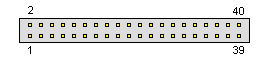
Назначение контактов разъема IDE
ATA=AT bus Attachment. Used at the PC, Apple Macintosh and some other computers
40 pin IDC male connector | Advanced Technology Attachment (ATA), is a standard interface for connecting storage devices such as hard disks and CD-ROM drives inside personal computers. Many terms and synonyms for ATA exist, including abbreviations such as IDE, ATAPI, and UDMA. ATA standards only allow cable lengths in the range of 450 to 900 mm, so the technology normally appears as an internal computer storage interface. It provides the most common and the least expensive interface for this application.
Each cable has two or three connectors, one of which plugs into a controller that interfaces with the rest of the computer system. The remaining one or two connectors plug into drives. Parallel ATA cables transfer data 16 or 32 bits at a time. One occasionally finds cables that allow for the connection of three ATA devices onto one IDE channel, but in this case one drive remains read-only (this type of configuration virtually never occurs). For most of ATA"s history, ribbon cables had 40 wires, but an 80-wire version appeared with the introduction of the Ultra DMA/66 standard. The 80-wire cable provides one ground wire to each signal wire. This reduces the effects of electromagnetic induction between neighboring wires and enables the 66 megabyte per second (MB/s) transfer rate of UDMA4. The faster UDMA5 and UDMA6 standards require 80-conductor cables. This was done to reduce crosstalk. Though the number of wires doubled, the number of connector pins remains the same as on 40-conductor cables. The connectors used for 80-way high speed ATA cables are not the same as the 40-pin connectors. Externally they look the same, but internally they are much more complicated, with a grounding rail along the body to earth all the extra shielding wires in the cable. If two drives attach to a single cable, the configuration generally sees one as a master and the other as a slave. The master drive generally shows up ahead of the slave drive when the computer"s operating system enumerates available drives. The master drive arbitrates access to devices on the channel. Because of this, latency-sensitive devices such as early CD-RW drives often benefitted from functioning as a master, and each channel must have a master in order to function properly. Note: Direction is Controller relative Devices (Harddisks). Developed by Western Digital, Conner & Seagate | ||||||||||||||||||||||||||||||||||||||||||||||||||||||||||||||||||||||||||||||||||||||||||||||||||||||||||||||||||||||||||||||||||||||||||||||||||||||||||||||||||||