

Партнерка на США и Канаду по недвижимости, выплаты в крипто
- 30% recurring commission
- Выплаты в USDT
- Вывод каждую неделю
- Комиссия до 5 лет за каждого referral
Supporting Information
Intrinsic Slow Charge Response in the Perovskite Solar Cells: Electron and Ion Transport
Jiangjian Shi, Xin Xu, Huiyin Zhang, Yanhong Luo, Dongmei Li, Qingbo Meng*
Key Laboratory for Renewable Energy, Chinese Academy of Sciences; Beijing Key Laboratory for New Energy Materials and Devices; Institute of Physics, Chinese Academy of Sciences, Beijing 100190, P. R. China
* Corresponding author *****@***ac. cn
1. Experimental details
Fabrication of perovskite solar cells with different structures and different deposition methods. The cells with structures of FTO/bl-TiO2/CH3NH3PbI3/Au, FTO/bl-TiO2/mp-TiO2 /CH3NH3PbI3/Au, FTO/bl-TiO2/CH3NH3PbBr3/Au, FTO/bl-TiO2/mp-TiO2/CH3NH3PbI3 /HTM/Au, FTO/bl-ZnO/CH3NH3PbI3/HTM/Au, and FTO/bl-SnO2/CH3NH3PbI3/HTM/Au were fabricated. The deposition methods including conventional sequential, two-step interdiffusion, one-step anti-solvent have all been applied as reported. For cell fabrication, 20 nm compact TiO2 layer and 150 nm mesoscopic TiO2 layer were spin coated onto the pre-cleaned FTO glass. And the perovskite absorber was then deposited onto the n-ETL layer with the above solution-processed methods. A 200 nm-thick Spiro-OMeTAD was used as the HTM layer, and an 80 nm-thick Au was evaporated as the back electrode.
Current-voltage (I-V) characterization for the cells. The cells with structures of FTO/bl-TiO2/mp-TiO2/CH3NH3PbI3/Au and FTO/bl-TiO2/mp-TiO2/CH3NH3PbI3/HTM/Au have been applied for I-V scanning measurements. For the HTM based cell, the scanning direction was 0-1.1-0 V; while for the HTM-free ones, the scanning direction was 0-0.85-0 V. The I-V data was recorded every 10 mV by a Keithley 2602 source meter and delay for 10, 100, 500 and 1000 ms, respectively. A sunlight simulator (Oriel Solar Simulator 91192, AM 1.5, 100 mW cm-2) calibrated with a standard silicon reference cell was used to give a one sun illumination. The steady-state output of the current for the HTM based cell has been recorded for 120 s at different bias voltages of -0.1, 0 and 0.8 V. For the normal I-V scanning measurements, no bias voltage has been applied at the cell before measuring. A negative (-0.9 or -0.5 V) and positive (1.1 V) bias voltages have also been applied before the cell was measured to investigate their influence, as discussed in the Supplementary Information.
Characterization with electrically modulated transient photocurrents. For the transient photocurrent (TPC) measurements, the current decay was excited by a 532 nm laser (Brio, 20 Hz) with duration of 4 ns and pulse fluence of about 20 nJ/cm2 (per pulse). A digital oscilloscope (Tektronix, DPO 7104, 50 Ω) was used to record the current decay process. A digital signal generator (Tektronix, AFG 3052C, 50 MHz) was used to give an external modulation at the cell. The signal generator was AC separated from the cell with two low-pass filters. For the DC modulated TPC measurement, the time resolution is 0.2 ns; while for the pulse modulated TPC measurement, the time resolution is 500 ns. For both measurements, the TPC signals were begun to be recorded 5 min after the DC or pulse voltage was applied. The cell was kept in dark when measuring. For bias illumination experiment, a white LED bias light was applied.
A series of perovskite solar cells with different structures and different film deposition methods were investigated, and the results discussed in this paper are considered to be universal and typical. The cycle time of the pulse laser is about 50 ms, much larger than the transport time of the cell; and the interference between different transient photocurrent signals is thus negligible.
Theoretical calculation of charge transport in the perovskite absorber. The charge transport inside the perovskite absorber has been analytically calculated with solving the one-dimensional transport equation (equation S1). To solvent this complicated equation, the dimension was first treated. And the dimensionless equation was finally analytically solved with separation of time (t) and space (x) in this equation. To investigate the influence of electric field, an approximately uniform electric field was also considered in the equation. As shown in equation (S1), the electron extraction velocity at n-ETL/perovskite interface (x=0) is described with SETL, which ranges from infinity to ultralow for different cell. For the back interface (x=L), the condition of perovskite/HTM is considered, that is, no free electrons transport across this interface. Because the transport equation is a linear equation, a monochromatic incident light with an absorption depth of x0 is considered. In a solar cell, the current density (J) can be described as Jn(0)+Jp(0). Since free holes can hardly transport across the n-ETL/perovskite interface, thus J=Jn(0)=qSETL∆n(0).
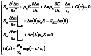 . (S1)
For the calculation of ion migration, a p-n+ semiconductor model was applied (Scheme 1), where the ions were only drifted under the electric field, and no ion diffusion was considered, as equation (S2) shows.
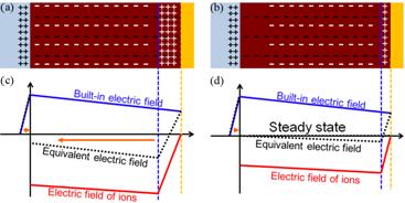
Scheme 1. Ion and electric field inside the cell.
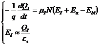 . (S2)
In equation (S2), N is the additional concentration of ion (vacancy). As the strength of the compensated electric field is comparable to that of the built-in field, the N should also be comparable to the hole density in the perovskite absorber (1014~1016 cm-3).
The mobility of ion migration can be calculated according to its definition as μ=v/E. And the vecocity can be calculated as
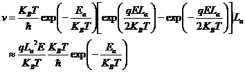 .
.
Thus, the mobility can be derived as  .
.
2. I-V hysteresis behaviors of perovskite cells
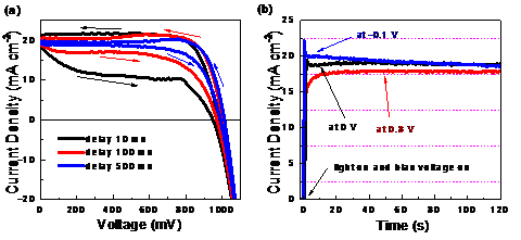
Figure S1. (a) I-V curves of the HTM based perovskite solar cell at different scanning rate, and (b) steady-state current output of the cell at different voltage. Before measuring, the cell was hold at 0 V. The scanning direction was 0 V-1.1 V-0 V.
As shown in Figure S1, when slowing the I-V scanning rate, the forward-scanning efficiency is significantly improved, but the backward-scanning efficiency is less influenced, which means that the averaged efficiency of the cell can be improved with slowing the scanning rate. When the cell was measured under a bias voltage of 0 V and 0.8 V, a stable current of 19 and 18 mA cm-2, respectively, can be output. But, when a negative voltage of -0.1 V is applied, a continuous decreasing of the current output was observed, which means that an opposite electric field inside the cell can gradually appear and enhance when the cell works under a negative voltage. All these results agree with the transient photocurrent results, and can be well explained with the ion migration and accumulation mechanisms.
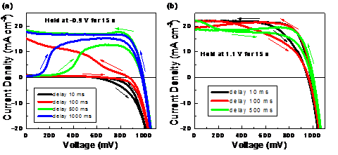
Figure S2. I-V curves of the HTM based perovskite cell held at (a) negative (-0.9 V) and (b) positive (1.1 V) bias voltage for 15 s before measuring. The scanning direction was 0 V-1.1 V-0 V.
When the cell was held at a negative or positive voltage for 15 s before I-V scanning measurement, interesting behaviors can be observed, as shown in Figure S2 and S3. For the negative voltage holding conditions, when the cell was then fast scanned, almost no current can be measured, as shown in Figure S2(a). When slowing down the scanning rate, an obvious increase in the current can be observed even when the bias voltage is increased. For the positive voltage holding conditions, an obvious decrease in the current can be observed when the cell was scanned under bias voltage, as shown in Figure S2(b). For the HTM-free cell, similar results were observed. All these results indicate the influence of external bias voltage on the equivalent electric field inside the cell and the evolution process of the electric field when the cell was scanning measured. Moreover, the evolution velocity of this electric field inside the HTM-free cell is much faster than that in the HTM based cell, as shown in Figure S2(b) and S3(b). All these results can also be well explained with the ion migration and accumulation mechanisms.
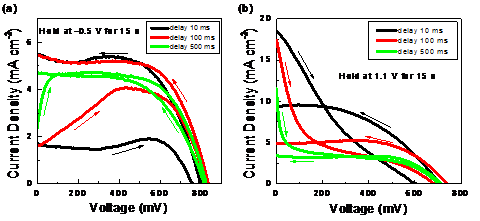
Figure S3. I-V curves of the HTM-free based perovskite cell held at (a) negative (-0.5 V) and (b) positive (1.1 V) bias voltage for 15 s before measuring. The scanning direction was 0 V-0.85 V-0 V.
3. Transient photocurrents results of CH3NH3PbBr3, silicon and HTM based cells
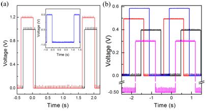
Figure S4. Transient photocurrent results of (a) CH3NH3PbBr3 and (b) silicon based cells under electrical pulse modulation. No hysteresis processes in the intensity of photocurrents were observed in these two types of cells.
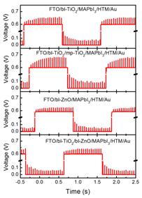
Figure S5. Transient photocurrent results of the CH3NH3PbI3 and HTM based perovskite cells with different ETLs under electrical pulse modulation. The hysteresis behaviors were observed in the TiO2 and ZnO based cells; while the hysteresis in the ZnO based cell is less serious.
4. Analysis of the transient charge processes in the cell
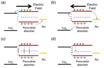
Figure S6. Schematic diagrams of transient charge processes in the HTM-free perovskite solar cell ((a) electron transport toward the TiO2 and hole transport toward the Au electrode, (b) electron transport toward the Au electrode and hole transport toward the TiO2, (c) charge recombination and (d) charge traps by interfacial or body defects). Blue dash lines depict the interfacial and body defects.
The general charge processes after the carrier is excited by a pulse laser are shown in Figure S6, including (a) positive or (b) negative charge transport from perovskite absorber to the contact materials, (c) charge recombination through interfacial or body defects and (d) charge trap by interfacial or body defects. In the transient photocurrent measurement, when photo-induced electrons transport toward the TiO2 and the sampling resistor, a positive photocurrent signal will appear (Figure S6(a)), whereas a negative signal would appear if the photo-induced electrons transport toward the Au electrode and the sampling resistor under a negative internal electric field (Figure S6(b)).
The recombination between photo-induced electrons and holes would also happen, as Figure S6(c) shows. However, this recombination can only lead to the decrease in concentration of free carriers and photocurrent, but cannot influence the direction of charge transport. The recombination would not change the occupancy conditions of defects.
Different from recombination, charge trap process would cause localized charge. However, this trap process itself would neither influence the direction of charge transport, but also decrease the concentration of free carriers, while the localized trap charge would induce a compensated electric field which can influence the charge transport. According to the negative transient photocurrent, it can be deduced that negative charge is localized at the TiO2/CH3NH3PbI3 interface. And when the bias voltage switches from low to high, the localized charge should be gradually decreased. For a semiconductor, the occupancy probability is determined by the Fermi energy. When the bias voltage switch from 0 to 0.4 V, the quasi Fermi energy of electron will be raised, increasing the occupancy probability. Thus, more negative charge is supposed to be localized at this interface, further lowering the transient photocurrent, which does not agree with the experiment results we observed. Moreover, when large negative bias voltage is applied at the cell, the difference in energy levels of the Fermi energy and trap states should be large enough and electric field in the absorber is very large, thus little negative charge can be localized. However, after the cell was held at -0.9 V for 15 s, even no photocurrent can be output, as shown in Figure S2(a). Thus, the mechanism of charge trap can hardly well explain all the experimental results we observed.
5. Time-dependent behavior of this hysteresis.
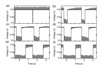
Figure S7. Transient photocurrent results of the perovskite solar cells, where the duration time of the external pulsed voltage at (-0.6 V) is (a) 0.02 s, (b) 0.4 s, (c) 0.6 s, (d) 0.8 s, (e) 1.2 s and (f) 1.4 s, respectively.
If the hysteresis behavior we discussed comes from the effect of static capacitance, this hysteresis process would always appear as long as the bias voltage changes with a constant rate. Figure S7 presents the relationship between transient photocurrents and varied duration of pulsed bias voltage. As shown, when the duration time of low voltage (-0.6 V) is only 0.02 s, no hysteresis behavior is observed. When the duration time increases to 0.4 s, this hysteresis behavior gradually appears, but almost no negative photocurrent signals is observed. Further increasing the duration time, negative signals appears and longer time is needed for the appearance of positive photocurrent, indicating a more serious hysteresis behavior. This time-dependent behavior implies that these hysteresis phenomena do not originate from the effect of static capacitance in the cell.
